

AXT InP 10H1Z00040021 indium phosphide substrate


$870.00
AXT InP 10H1Z00040021 Semiconductor Substrate.
***MPN 10H1Z00040021
***OEM AXT Inc
***SKU*** 30447
1 in stock
CompareProduct Description
AXT InP 10H1Z00040021 – Indium Phosphide (InP) Semiconductor Substrate – Research/Grade
A high-quality indium phosphide (InP) semiconductor substrate from AXT (American Xtal Technology) , a leading manufacturer of compound semiconductor materials. The 10H1Z00040021 is a specialized substrate designed for epitaxial growth and device fabrication in optoelectronic, RF/microwave, and high-speed electronic applications. InP offers superior electron mobility and direct bandgap properties essential for lasers, photodetectors, HEMTs, and HBTs.
🔍 Key Specifications:
📡 Material & Specifications:
-
Manufacturer: AXT (American Xtal Technology)
-
Part Number: 10H1Z00040021
-
Material: Indium Phosphide (InP) – III-V compound semiconductor
-
Type: Semiconductor substrate (for epitaxial growth)
-
Diameter: Typically 2″, 3″, or 4″ – verify specific size from part number/labeling
-
Orientation: (100) or miscut – typical for InP device fabrication
-
Dopant: Undoped (semi-insulating) or Fe-doped – verify by part number
-
Resistivity: High (semi-insulating) for RF devices, or low for optoelectronic
-
Surface Finish: One side polished (epi-ready), one side etched/ground
-
Thickness: Standard substrate thickness (350–650 µm typical)
🔧 Physical Specifications:
-
Shape: Circular wafer
-
Edge: Ground/flat (primary flat or notch for orientation)
-
Packaging: Originally in cleanroom-grade container (if present)
-
Condition: Surplus – visually inspected, unopened container if sealed
⚙️ Why InP Substrates are Critical:
🔬 Superior Material Properties:
Indium phosphide offers:
-
High electron mobility – faster devices, higher frequencies
-
Direct bandgap – efficient light emission/detection
-
High breakdown field – high-power RF devices
-
Thermal conductivity – better than GaAs for power applications
📡 Key Applications:
-
Optoelectronics: Laser diodes (telecom 1310/1550nm), photodetectors, modulators
-
RF/Microwave: HEMTs, HBTs for mm-wave, 5G, radar
-
High-speed electronics: Digital circuits, mixed-signal ICs
-
Photovoltaics: High-efficiency multi-junction solar cells
🏭 Semiconductor Manufacturing:
InP substrates are used for:
-
Epitaxial growth (MBE, MOCVD) of device layers
-
Device fabrication – lithography, etching, metallization
-
Research & development – new materials, device concepts
🛠️ Potential Applications (If Suitable):
🔬 Research & Development:
-
Epitaxial growth experiments – test new material combinations
-
Device prototyping – fabricate test structures
-
Material characterization – study InP properties
📡 Optoelectronic Device Fabrication:
-
Telecom lasers – 1310nm/1550nm edge-emitting or VCSELs
-
Photodetectors – PIN, APD for fiber optic receivers
-
Modulators – electro-absorption, Mach-Zehnder
📶 RF/Microwave Devices:
-
HEMTs – low-noise amplifiers, power amplifiers
-
HBTs – high-linearity amplifiers, oscillators
-
mm-wave ICs – 5G, automotive radar, satellite comms
🔋 Photovoltaics:
-
Multi-junction solar cells – space and concentrated PV
-
Tandem cells – with GaAs, InGaAs layers
🧪 Educational Use:
-
University semiconductor labs – hands-on processing experience
-
Training – epitaxy, lithography, device fabrication
| Weight | 1 lbs |
|---|---|
| Dimensions | 8 × 6 × 4 in |
Related products

Semiconductor Processing Equipment

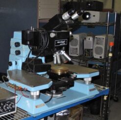
Semiconductor Processing Equipment
Semiconductor Processing Equipment
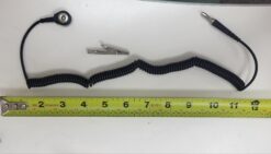
3M 2210 Static Control Ground Cord for Charge-Guard Wrist Band


