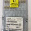
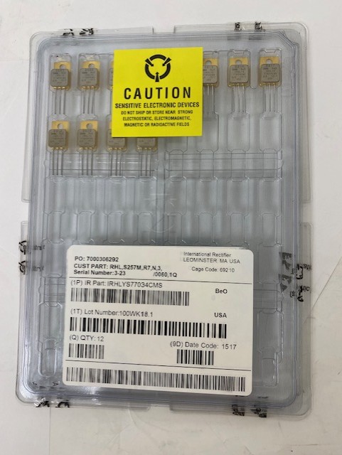
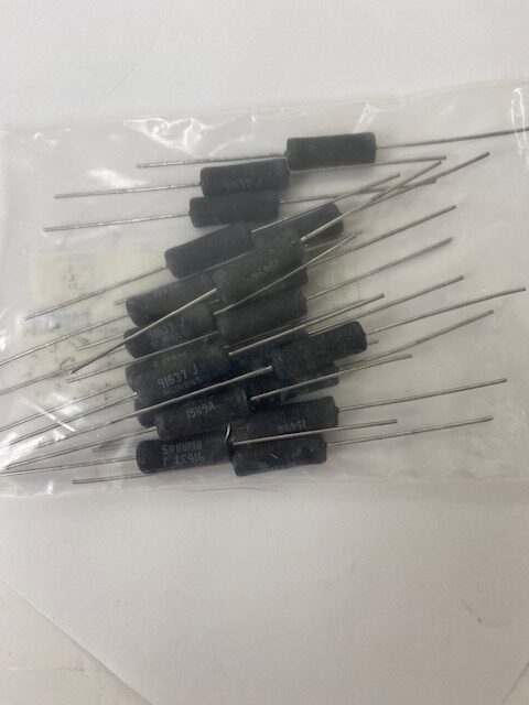
International Rectifier IRHLYS77034CMSCS MOSFET – LOT OF 12
Original price was: $4,000.00.$3,300.00Current price is: $3,300.00.
1 in stock
Compare🛰️ Overview & Applications
This device is a 60 V, N-channel, hermetically‑sealed MOSFET in a TO‑257AA package, specifically manufactured for space and other high-radiation environments. It offers:
-
Total Ionizing Dose (TID) tolerance to 100 krad(Si), with SEE immunity up to ~85 MeV⋅cm²/mg
-
Hermetic sealing, light weight, and simple gate drive (5 V CMOS/TTL compatible)
-
High ESD rating: Class 1B per MIL‑STD‑750 Method 1020
Typical use cases include PWM circuits and current boosting in satellite, avionics, and defense applications.
🔧 Key Specifications
| Parameter | Value |
|---|---|
| BVDSS (Drain‑Source Voltage) | 60 V |
| RDS(on) (VGS = 4.5 V, 25 °C) | 0.045 Ω |
| Continuous Drain Current | 20 A (package-limited) |
| Gate Charge (Qg) | ~34 nC |
| Switching Times (Turn-on /off) | 26 ns / 60 ns |
| Single Pulse Avalanche Energy | 98 mJ |
| dv/dt Capability | 6.9 V/ns |
| Power Dissipation | 75 W (at Tc=25 °C) |
| Operating Temperature | –55 °C to +150 °C |
| Leakage Currents | <1 µA (zero gate bias) |
Radiation performance remains stable post-irradiation to 300 krad(Si), with minimal shifts in threshold voltage, breakdown voltage, and on-resistance
| Weight | 2 lbs |
|---|---|
| Dimensions | 9 × 6 × 3 in |
Related products


Integrated Circuits and Op Amps
ACTEL APA300-BG4561 FPGA ProASICPLUS Family 300K Gates – LOT OF 9